Farrell55
Banned
380 is wrong, ms confirmed via DF a 360 mm2 dieI don’t think there is any source but all “leaks” points to a smaller chip from Sony.
The same Foxconn guy that said Xbox was aground 380mm2 said PS5 is around 350mm2.
380 is wrong, ms confirmed via DF a 360 mm2 dieI don’t think there is any source but all “leaks” points to a smaller chip from Sony.
The same Foxconn guy that said Xbox was aground 380mm2 said PS5 is around 350mm2.
Well it is now wrong but the first two dies picks from Phil was definitely > 380mm2.380 is wrong, ms confirmed via DF a 360 mm2 die
Ok, I think I got it.You can read from the first 10GB at 320bits.
The other 6GB can only be read at 192bits.
The first 10GB will have data that is striped across all of the memory modules to achieve 320bits.
The last 6GB will have data that is striped only across all the higher capacity chips to achieve 192bits.
This is because the higher capacity chips have a memory space (the extra capacity) that does not exist in the lower capacity chips and therefore cannot be striped with them. But this limitation only occurs when you use the extra capacity on the higher capacity chips, therefore if you stick to the first half of the memory space you can read across both the lower and higher capacity chips at once.
I think both will have 16GB, but Sony will be using a 256bit bus.
Okay so you Expect it can be smaller based on this guy, it will be very exciting to see whats Sony will deliver in the end
Ment to say what’s on the screen. I just don’t see a difference at all. Might need a 4K tv to see the difference? Is what I was asking.too see what 4k looks like you need a 4k screen
I think that PS5 will have 20GB GDDR6 (10 modules and 320bit bus) so the MS's higher bandwidth is gonna be sustained for PS5 and 4GB of DDR4 for OS. That is why BB article points to higher than expected BOM as the RAM prices soared lately.
I dont think that on the Photos was a 380 mm2 die, i think people guessed it wrongWell it is now wrong but the first die picks from Phil was definitely > 380mm2.
My take was that it wasn't both it's congruently but if they were to run the chip flat out at 16bit it would perform 25 tf.I read it.
12tf of normal stuff and another 13tf from RT hardware = it's like 25tf when running RT games.
Awesome. Good to see DF get first coverage of SeX and tell gamers this:
"Without hardware acceleration, this work could have been done in the shaders, but would have consumed over 13 TFLOPs alone," says Andrew Goossen. "For the Series X, this work is offloaded onto dedicated hardware and the shader can continue to run in parallel with full performance. In other words, Series X can effectively tap the equivalent of well over 25 TFLOPs of performance while ray tracing."
Well it is now wrong but the first two dies picks from Phil was definitely > 380mm2.
Anubis is no longer doing, it may be the development machine code Arden should not have been unexpected to be the version to be released and Arden is moving faster, obr is still in the early stages of verification and Arden is more than one size larger than the OBR (350 vs 300 mm2)
Ok, I think I got it.
We have 4 1GB chips and 6 2GB chips for a total of 10 chips and 16 GBs. When reading from the first GB of each chip, we can use them all at the same time getting 576 GB/s. But when you allocate data to the second GB of the 2GB chips, you can't distribute that data among the 1GB chips because they don't have that extra space so your speed when accessing that data is limited to 6/10s of the maximum theoretical speed, which is approximately 340something GB/s. Is that it?
What total bandwidth would that produce?
Well it is now wrong but the first two dies picks from Phil was definitely > 380mm2.
Translation please what am I looking at?He said XSX was 350 and PS5 was 300.
looks like he was on the nose
https://pttweb.tw/s/3We5x
People guessed wrong because they were using imprecise measurements. The die size didn’t change.
Perhaps Lisa Su's Ryzen style PC 4K GPU disruption claim could be true. "80 CU RDNA 2" Big Navi perhaps.Yeah that's what came to mind, EVEN if it is not 100 FPS (which it is), you're still looking at...
- Native 4K/60FPS.
- 50% more particle effects than PC Ultra. (can be demanding at times).
- Better volumetric lighting than PC Ultra. (demanding).
- New tech: Contact-hardening shadows. (demanding).
- Screen-space Ray Traced Global Illumination. (demanding).
This already is better than what RTX 2080 Ti offers, we haven't looked at it being 100FPS as well.
Looks like they optimized the Unreal 4 engine even more and maybe the RDNA 2 GPU architecture is 50% more efficient because that with the 12 TFs = more performance than the RTX 2080 Ti.
team github's suicide note.Translation please what am I looking at?
and I meant yes you do need a 4K tv or monitor. They just changed the resolution and fps on GOW5. As far as I knowMent to say what’s on the screen. I just don’t see a difference at all. Might need a 4K tv to see the difference? Is what I was asking.
why wouldn't it? since when do people think more options are a bad thing? you can use the official battery pack, you can use yoir own AA batteries or you can use third party offerings.
I have battery packs made by Energizer for example, they come with a charge dock and last about 10h... cheap, long enough battery life and you just put the controller in the charge dock after you're done playing.
before that I used high quality AA rechargables.
Well it is now wrong but the first two dies picks from Phil was definitely > 380mm2.
Yeah. That is called reification, as previous guesstimates were based on 16nm value comparisons with 5700 series CU size I think and were wrong for all APU guesses since the beginning.People were guessing wrong on the recent die pic as well. No one estimated 360mm until the official numbers were reached.
People have a hard time estimating period.
Translation please what am I looking at?
OBR 310mm2 could get us 44CU at 2.0Ghz+ =11.2TF-11.6TFteam github's suicide note.
I believe the 380mm2 estimation was based in the memory chip size.Yeah. That is called reification, as previous guesstimates were based on 16nm value comparisons with 5700 series CU size I think and were wrong for all APU guesses since the beginning.
Nope they're exactly the same chip.I believe the 380mm2 estimation was based in the memory chip size.
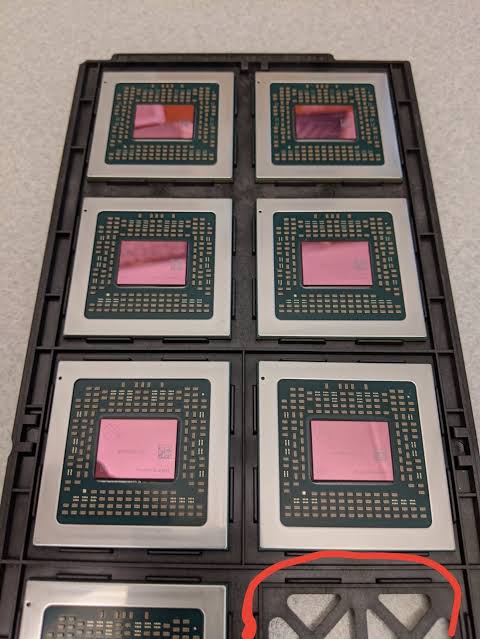
The new chip showed yesterday is a bit smaller than the one showed by Phil in December.


They are not.Nope they're exactly the same chip.
old one was hardware sample and new one is the chip you will find in Finished ProductOld chip.
New chip.
They are not.
They even changed what is write in the chip.
I think AquariusZi was referring to die category sizes. Something like "Arden is more than a size larger than Oberon".He said XSX was 350 and PS5 was 300.
looks like he was on the nose (ok so 360 vs 350 much closer than anyone else and he had no photos like we did)
https://pttweb.tw/s/3We5x
People guessed wrong because they were using imprecise measurements. The die size didn’t change.
I think changing the die size in a couple of months isnt even possible, also whats the reason that they have changed the die size?Old chip.
New chip.
They are not.
They even changed what is write in the chip.
The previous chip was probably a ES for Project Scarlett.
there's nothing confirmed, I think this comes from a guy who accurately ""leaked"" the dimensions of the Series X's SoC, he also had measurements for the PS5's SoC
Nope only 8K is missing. That Phil Spencer profile pic from twitter (1st one) is photoshopped to suppress what is written on the die and also an engineering sample. But the dies are the same, as can be seen from the protrusions around the die is exactly matching.Old chip.
New chip.
They are not.
They even changed what is write in the chip.
The previous chip was probably a ES for Project Scarlett.
Flex on um chip vs realityOld chip.
New chip.
They are not.
They even changed what is write in the chip.
The previous chip was probably a ES for Project Scarlett.
Nope.Nope only 8K is missing. That Phil Spencer profile pic from twitter (1st one) is photoshopped to suppress what is written on the die and also an engineering sample. But the dies are the same, as can be seen from the protrusions around the die is exactly matching.
Ok, I think I got it.
We have 4 1GB chips and 6 2GB chips for a total of 10 chips and 16 GBs. When reading from the first GB of each chip, we can use them all at the same time getting 576 GB/s. But when you allocate data to the second GB of the 2GB chips, you can't distribute that data among the 1GB chips because they don't have that extra space so your speed when accessing that data is limited to 6/10s of the maximum theoretical speed, which is approximately 340something GB/s. Is that it?
MotherOfGod.jpgYeah that's what came to mind, EVEN if it is not 100 FPS (which it is), you're still looking at...
- Native 4K/60FPS.
- 50% more particle effects than PC Ultra. (can be demanding at times).
- Better volumetric lighting than PC Ultra. (demanding).
- New tech: Contact-hardening shadows. (demanding).
- Screen-space Ray Traced Global Illumination. (demanding).
This already is better than what RTX 2080 Ti offers, we haven't looked at it being 100FPS as well.
Looks like they optimized the Unreal 4 engine even more and maybe the RDNA 2 GPU architecture is 50% more efficient because that with the 12 TFs = more performance than the RTX 2080 Ti.
nah it's the same chipNope.
There are pics lol

PS5 won’t have more CUs than Xbox.
They are basically using a smaller die.
So 48? 50?
Navi 21 Guesses were also very wrong!I think AquariusZi was referring to die category sizes. Something like "Arden is more than a size larger than Oberon".
MrFox from Beyond3d also came quite close to the 360mm² measurement with his estimate.
If this is true, then Oberon would be ~300mm², so maybe like 310mm². Also of note, AquariusZi leaked the Navi 21 die size at 505mm². That's without a CPU on die in comparison to XSX's 360mm² with a CPU. Assuming this is accurate, and a 360mm²(maybe ~300mm² GPU?) can "already deliver very, very similar performance to an RTX 2080", then what kind of monster is that Navi 21 chip?
'Backwards compatible with EVERY Playstation console'
So what's everyone thinking on this now that SeX is revealed?
I think whoever put this has heard TF number but calculated his own opinion of CU and GHz.
nah it's the same chip
why because they romved 8k logo and project scarlet ? like i said old one was hardware sample for testing and the new one is what you will find in a finished productIt is the same socket lol
Capacitors and package will be similar.
The chip itself are not the same.
'Backwards compatible with EVERY Playstation console'
Yeah nah. Tales from ass.
 ?
?Yeap they are different chips.why because they romved 8k logo and project scarlet ? like i said old one was hardware sample for testing and the new one is what you will find in a finished product
'Backwards compatible with EVERY Playstation console'
Yeah nah. Tales from ass.
So what they are gonna add that missing 20mm2 back on the chip to please the mm2 measurers and CU counters, and along the way make it 56 CUs with 4 disabled so 60 in total to also validate GitHub as a bonus?Yeap they are different chips.
BTW it is not clear the chip showed yesterday will be the one to go into production.
For a November releases the final chips are usually produced after June.
probably still chill and relax in bathub while watching TLOU2 and GoT poster hanging on ceilingLast time this round, Sony went about nonchalantly announcing ps4 specs in Feb, while there were rumors and leaks and hype about what's in xbox. Remember we went as far as rumoring xbox have a 8 cores intel cpu?
I can picture in Sony hq now, scrambling which parts of PS5 to panic boost so it looks comparable on paper.
Xbsx specs are totally great, well beyond my next gen expectations.
Sony where art yoz?
Odd that the zip code on that is 16-512. Its not a zip code at all. Only thing I can think it means is 16GB with a 512 bus. But no current cards use a 512 bus. They are all 352 or 256.Older amd cards like the 290x did.
Cremated and then buried for a safe measure.What I wanna know is if Team Github is dead
RIP Team GithubCremated and then buried for a safe measure.

