The Foxconn leaks had too many little details right. Even the the pair of neon Joy Con. At 16nm, the clock speeds aren't too far fetched from the realm of possibility.Then how does that explain Eurogamer's leaked speeds being "final for launch"?
-
Hey, guest user. Hope you're enjoying NeoGAF! Have you considered registering for an account? Come join us and add your take to the daily discourse.
You are using an out of date browser. It may not display this or other websites correctly.
You should upgrade or use an alternative browser.
You should upgrade or use an alternative browser.
The Curious Case of the Switch Foxconn Leak (Now a hardware fanfiction thread)
- Thread starter Cerium
- Start date
Skittzo0413
Member
The Foxconn leaks had too many little details right. Even the the pair of neon Joy Con. At 16nm, the clock speeds aren't too far fetched from the realm of possibility.
Yeah it may be right but we have no idea if the tested clock speeds are for developers to use, or even for all of the cores. The leaker speculated 16nm based on the speeds, not the other way around. We won't know for sure the retail speeds or process node just from these pictures.
The Foxconn leaks had too many little details right. Even the the pair of neon Joy Con. At 16nm, the clock speeds aren't too far fetched from the realm of possibility.
I asked before, but you seem so sure that something is now confirmed, so I will ask again, what exactly are these picture here confirming without a doubt?
ShadowFox08
Member
Yeah it may be right but we have no idea if the tested clock speeds are for developers to use, or even for all of the cores. The leaker speculated 16nm based on the speeds, not the other way around. We won't know for sure the retail speeds or process node just from these pictures.
The RAM should be the easiest thing to tell just from looking, right?
Yeah we likely won't know clockspeeds until maybe first week of launch at the earliest.
Yeah it may be right but we have no idea if the tested clock speeds are for developers to use, or even for all of the cores. The leaker speculated 16nm based on the speeds, not the other way around. We won't know for sure the retail speeds or process node just from these pictures.
I've leaned toward the Foxconn clock speeds being true for weeks now.I asked before, but you seem so sure that something is now confirmed, so I will ask again, what exactly are these picture here confirming without a doubt?
The GPU upclock could have been decided after DF leak. We're talking about 150MHZ more, it's absolutely possible if temperatures aren't an issue. Pascal was just speculation from the foxconn leaker so it can be 921MHZ but not Pascal or 16nm (although it would make more sense to have a clock that high with 16nm, but then again, it's a custom chip, it can be 16nm, 921MHZ, but not Pascal, or it could be all three).The Foxconn leaks had too many little details right. Even the the pair of neon Joy Con. At 16nm, the clock speeds aren't too far fetched from the realm of possibility.
The weird thing is the CPU clockspeed. We've seen in the leaked documents that there are 3 CPU cores for games, which means that one of them is being reserved for the OS. Thraktor speculated that the higher clock could be for the one core dedicated to the OS. It would make sense in a way, because both the foxconn leaker and df would be right, the CPU clock varies between the three cores for games and the single core for the os, while the GPU upclock is certainly reasonable and there's no reason for Nintendo not to do that if thermal figures allow for it. It's still a good 20% more performances that can help in every scenario.
The only reason i'm not 100% convinced of this is that i don't know if it makes sense to test the clockspeed used for the OS for 8 days with a Vulkan demo, which is something computationally intensive, AND with the GPU clock at the max speed, because no way that it runs at 921MHZ during the os browsing. Wouldn't they also test the 1.02GHZ clock for the other 3 cores?
two more photo
Maybe using this picture vs. this:

could give some hint?
Although I think the margin of error might be too big.
I was 100% joking if that was unclear.I asked before, but you seem so sure that something is now confirmed, so I will ask again, what exactly are these picture here confirming without a doubt?
Wouldn't the fact that these chips were fabbed in July indicate the Eurogamer clocks might be more in line with what we end up with? (At least according to post in other thread, I have no idea if the above is accurate).
At any rate it looks like they made a really efficient use of the space available in their spec. Bodes well for the future of the Nviendo partnership.
At any rate it looks like they made a really efficient use of the space available in their spec. Bodes well for the future of the Nviendo partnership.
ShadowFox08
Member
Wouldn't the fact that these chips were fabbed in July indicate the Eurogamer clocks might be more in line with what we end up with? (At least according to post in other thread, I have no idea if the above is accurate).
At any rate it looks like they made a really efficient use of the space available in their spec. Bodes well for the future of the Nviendo partnership.
Not necessarily. The july dev kits could have been made before july
frankie_baby
Member
Wouldn't the fact that these chips were fabbed in July indicate the Eurogamer clocks might be more in line with what we end up with? (At least according to post in other thread, I have no idea if the above is accurate).
At any rate it looks like they made a really efficient use of the space available in their spec. Bodes well for the future of the Nviendo partnership.
Just because the chip was fabbed in july doesn't mean in necessarily made it into a dev kit in july
Buggy Loop
Member
Wouldn't the fact that these chips were fabbed in July indicate the Eurogamer clocks might be more in line with what we end up with? (At least according to post in other thread, I have no idea if the above is accurate).
At any rate it looks like they made a really efficient use of the space available in their spec. Bodes well for the future of the Nviendo partnership.
How do you know they were fabbed in july?
frankie_baby
Member
How do you know they were fabbed in july?
1629 = 2016 week 29
ShadowFox08
Member
How do you know they were fabbed in july?
There's a code that says 1629, which indicates 2016 and the 29th week which is around july apparently.
http://www.neogaf.com/forum/showthread.php?t=1345524
Don't forget that the clocks leaked by Eurogamer were communicated much later than July. I don't see how the final chips were fabricated in July and Nintendo would communicate much lower clocks in the Fall only to revise them a month or two later. Doesn't make too much sense.
Skittzo0413
Member
Don't forget that the clocks leaked by Eurogamer were communicated much later than July. I don't see how the final chips were fabricated in July and Nintendo would communicate much lower clocks in the Fall only to revise them a month or two later. Doesn't make too much sense.
Yeah I'll agree with that. The only thing which might make sense is Nintendo opting to increase the clock speeds after launch, though I don't know why.
Or Eurogamer's source was wrong/fake. Which seems unlikely because they have a great track record.
tomwhite2004
Member
Or Eurogamer's source was wrong/fake. Which seems unlikely because they have a great track record.
Eurogamer actually said they had multiple sources which makes me more inclined to go with what they said.
blu
Wants the largest console games publisher to avoid Nintendo's platforms.
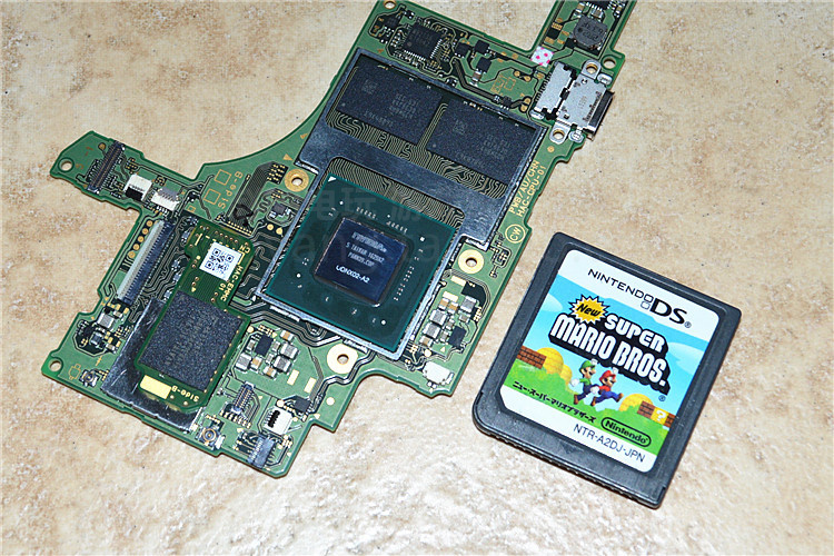
Boy, this is one sexy piece of hw.two more photo
Also, checking the baidu pics - heatpipe + fan setup is very similar to the Shield. We need proper measure estimates to tell how big is Switch's. Other than that, eMMC module is trivial, but the ROM cart iface is surprisingly wide.
Or eurogamer sat on that info for months, the fact that they received the info (for example) in late september/early october doesn't mean that the kits with those clocks were shipped just before that. They could have been around for months and months, and even be largely based on the stock tx1 with some customizations (which is actually what DF said in their summer article about NX using tegra iirc). Not to say that eurogamer's clocks are certainly wrong (read my previous post on the matter), but i don't think this tells us anything new, really.Yeah I'll agree with that. The only thing which might make sense is Nintendo opting to increase the clock speeds after launch, though I don't know why.
Or Eurogamer's source was wrong/fake. Which seems unlikely because they have a great track record.
In any case, it's obvious that we can't just dismiss the foxconn leak either. The guy was spot on about everything, doesn't make sense that he made up all the shit about the clocks.
Or eurogamer sat on that info for months, the fact that they received the info (for example) in late september/early october doesn't mean that the kits with those clocks were shipped just before that. They could have been around for months and months, and even be largely based on the stock tx1 with some customizations (which is actually what DF said in their summer article about NX using tegra iirc). Not to say that eurogamer's clocks are certainly wrong (read my previous post on the matter), but i don't think this tells us anything new, really.
In any case, it's obvious that we can't just dismiss the foxconn leak either. The guy was spot on about everything, doesn't make sense that he made up all the shit about the clocks.
There were not new kits with the clocks, the clocks were communicated to the devs as target specs.
So July 18th to the 25th for this chip.
First thing I can see that makes me really puzzled is using 2 ram chips, this would indicate 128bit memory bus, but thraktor in the other thread thinks he might have figured out the model number and those are 32bit chips for 64bit bandwidth. You think you'd just use 1 64bit chip for this.
The soc is a socket based chip? Its' area is much bigger than x1 in Tegra but the die seems to be about the same size, of course 20nm and 16nm are pretty much the same size so this doesn't really help us.
I would say that this isn't pascal, though it could still be 16nm, meaning it's about the same thing. X1 isn't a standard maxwell chip and was the basis for pascal anyways.
Foxconn leak was right, that much is definitely confirmed here. I think western devs could have asked for more performance from the cpu, this would push Nintendo to test higher clocks. I think until we understand why they would test the cpu at such a high clock, we should ignore both eurogamer and foxconn clocks as definitive, it's possible that they went with a clock between them as well. Though I do think the Foxconn clocks are more likely.
The 32-bit RAM units are pretty much confirmed, in the other thread we have read off the letters and numbers on the RAM units and it exactly matches this piece of hardware, which Thraktor said was 32-bit per module: http://www.samsung.com/semiconducto...e-dram/low-power-ddr4/K4F6E304HB-MGCH?ia=3107So July 18th to the 25th for this chip.
First thing I can see that makes me really puzzled is using 2 ram chips, this would indicate 128bit memory bus, but thraktor in the other thread thinks he might have figured out the model number and those are 32bit chips for 64bit bandwidth. You think you'd just use 1 64bit chip for this.
The soc is a socket based chip? Its' area is much bigger than x1 in Tegra but the die seems to be about the same size, of course 20nm and 16nm are pretty much the same size so this doesn't really help us.
I would say that this isn't pascal, though it could still be 16nm, meaning it's about the same thing. X1 isn't a standard maxwell chip and was the basis for pascal anyways.
Foxconn leak was right, that much is definitely confirmed here. I think western devs could have asked for more performance from the cpu, this would push Nintendo to test higher clocks. I think until we understand why they would test the cpu at such a high clock, we should ignore both eurogamer and foxconn clocks as definitive, it's possible that they went with a clock between them as well. Though I do think the Foxconn clocks are more likely.
Except it really doesn't. The last line is just the dimensions of the chip and the line before it, that second digit doesn't look like a 4 and we can't tell if the last two are 80, 30, or 33.The 32-bit RAM units are pretty much confirmed, in the other thread we have read off the letters and numbers on the RAM units and it exactly matches this piece of hardware, which Thraktor said was 32-bit per module: http://www.samsung.com/semiconducto...e-dram/low-power-ddr4/K4F6E304HB-MGCH?ia=3107
ShadowFox08
Member
What do you guys make of this?
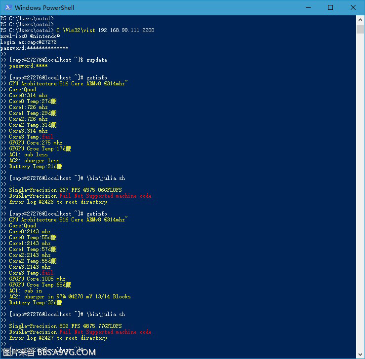
If we assume those are 2 different power profiles, that's one hell of a CPU upclock.What do you guys make of this?
If we assume those are 2 different power profiles, that's one hell of a CPU upclock.
If it's real, the second clocks are likely debug testing and not clocks for games, just topping out the soc, which the X1 is capable of.
I don't know what cpu flops are on the clock given, but the gpu would be doing 281gflops and would mean that the cpu would have to make up the difference to hit that 375gflops number.
The double precision isn't possible on Tegra iirc so that lines up, the big wtf here though is 512 cores, maybe it is a very early iteration for next year, that they are doing early testing on? We have no rumors or leaks to support such a massive jump from July and would put this on par with current gen consoles easily at 1tflops gpu power and 1.7tflops mixed precision, with a maxwell/pascal performance advantage.
A Volta powered switch is a nice dream I guess.
dampflokfreund
Banned
As pointed in the other thread the gap between GFLOPS doesn't match the gap between GPU clocks.
Isn't it possible that the chip can deactive/pause shader cores in low power mode?
If the clocks and gflops counts are true, we are looking at roughly xbox one power in fullspeed mode which would be a lot more powerful than we expected.
I wouldn't get my hopes up though.
calc84maniac
Member
No, the problem is that the gap is too small. That would just make the gap larger.Isn't it possible that the chip can deactive/pause shader cores in low power mode?
Isn't it possible that the chip can deactive/pause shader cores in low power mode?
If the clocks and gflops counts are true, we are looking at roughly xbox one power in fullspeed mode which would be a lot more powerful than we expected.
I wouldn't get my hopes up though.
That would work if the gap would be too big. But here the lower value is too high.
Deactivating shaders in the high performance/docked mode doesn't really make sense since it seems to max everything else.
And like z0m1ie just pointed out it has 512 cores which there is no chance of. Looks fake to me.As pointed in the other thread the gap between GFLOPS doesn't match the gap between GPU clocks.
ecosse_011172
Junior Member
Eurogamer said:Documentation supplied to developers along with the table above ends with this stark message: "The information in this table is the final specification for the combinations of performance configurations and performance modes that applications will be able to use at launch."
It wasn't the opinion of a developer, it was written in official documentation and reported on in December 2016.
That's what makes the foxconn fanfic performance bump very, very unlikely to me.
It wasn't the opinion of a developer, it was written in official documentation and reported on in December 2016.
That's what makes the foxconn fanfic performance bump very, very unlikely to me.
Well "at launch" has always struck me as a odd thing to mention in that line. Could suggest a consideration of upping performance later.
No matter what anyone thinks about the likelihood of certain clocks in retail hardware everyone by now surely has to accept that the Foxconn info is solid. So Nintendo certainly wanted to know that the SoC could run at a combined 921mhz/1785mhz frequency for whatever reason. A bump in performance is just as logical or more than any other theory we've heard, far from fan fiction.
And like z0m1ie just pointed out it has 512 cores which there is no chance of. Looks fake to me.
yeah under further calculating (while not on a phone) the later clocks are completely off, the single precision is completely wack, the GPU alone would do 1tflop yet it is under that with all 516cores? It's a good thing someone like me doesn't create a fake, it would be easy enough to get the calculations right and then we'd all be stumped, especially at this point in the product's cycle where tear downs are popping up.
Well "at launch" has always struck me as a odd thing to mention in that line. Could suggest a consideration of upping performance later.
No matter what anyone thinks about the likelihood of certain clocks in retail hardware everyone by now surely has to accept that the Foxconn info is solid. So Nintendo certainly wanted to know that the SoC could run at a combined 921mhz/1785mhz frequency for whatever reason. A bump in performance is just as logical or more than any other theory we've heard, so think its silly to call it fan fiction personally.
We got that title because of another thread that was created about the enhanced dock, they linked here, so it drew attention to our conversation about a dock that is on par with Scorpio, that isn't something anyone who didn't read the foxconn leak and understood it was ready for, and made us look like we were just grasping at straws.
The "enhancer" is as real as we could hope from unofficial channels, I mean unless this person leaked all of this information just to in the end create an elaborate hoax that requires a certain amount of technical knowledge. I think it's safe to assume the device exists as a prototype and the rumors floating around do help confirm it. We do have to wait before we know if it will ever hit market, but it is an interesting device none the less.
It wasn't the opinion of a developer, it was written in official documentation and reported on in December 2016.
That's what makes the foxconn fanfic performance bump very, very unlikely to me.
Reality isn't something we choose to accept, the clocks and test existed, we don't know 100% why, and leaning on a document from August/September is a bad idea IMO, especially with Nintendo's willingness to listen to developers even so far as to add RAM to the device. We can find out the fact very soon either way, so there is no point in falling on a dagger on either side of the fence, just stay on it for now and jump down when you know its safe.
Cuningas de Häme
Member
Yeah I understand why it happened, still silly IMO. Shouldn't even post in a thread without reading first, let alone rename a thread based on nothing more than a assumption.
Well, most of the people in this forum seem to read only the name of the topic, and mods often take just a cursory look on the thread (can't blame them, it is a living Hell to try to moderate something this big, wouldn't do that job myself). And when people are spouting weird stuff all over the place creating hyberboles and whatnot, that's what mods see. The real discussion drowns under the "special experts".
Better to have this name and keep the topic open, maybe it even has stopped some of the more notorius posters actively trying to "temper fanboy expectations"...
I wouldn't accept the Eurogamer stuff as gospel, they get their info from leakers too and leakers are a nasty bunch. Never know what they're up to. Eurogamer works with the info they're given and they are often quite reliable, but they cannot be 100% right everytime.
We'll see what the Switch has eaten in the next couple of weeks, I am sure there's some tech sites ready to tear the Switch open and reveal it's seedy underbelly to the world.
It will be fun to see what the truth is. I love the Switch already and it has so many games revealed that I personally want, and I can play them whenever wherever. That is a huge leap in the console industry, and I think Nintendo will keep doing this for generations.
It just fits Nintendo so well, a mobile console.
Higher rez pics just came up, it's the model tag is (?)DNX02-A2.
I would say that this isn't pascal, though it could still be 16nm, meaning it's about the same thing. X1 isn't a standard maxwell chip and was the basis for pascal anyways.
On ArsTechnica they were reading a bit more into the model tag and came to a similar conclusion as z0m3Ie
"If this Nvidia chip is legitimate, then its printed code is interesting, because it contains a code label of "UDNX02-A2." We know the Switch is set to contain a Tegra chip, and we had been led to believe that this would be much like the X1 found in Nvidia's Shield devices. But this "A2" designation, unlike the "A1" printed on existing X1 chips, could mean we're getting a significant change to the design.
That may very well be a shrink to a 16nm process, or we could actually be getting a surprise bump from the older Maxwell architecture to the newer Pascal. The latter seems rather unlikely, however, based on known Switch specifications that developers are designing to." https://arstechnica.com/gaming/2017/02/is-this-what-the-nintendo-switchs-insides-look-like/
On ArsTechnica they were reading a bit more into the model tag and came to a similar conclusion as z0m3Ie
And their theory falls apart when you see that the Tegra in the new Shield also has an A2 code:

And their theory falls apart when you see that the Tegra in the new Shield also has an A2 code:
Luck has it, I don't rely on it. I believe it is a derivative of x1, it is custom and I'm wondering if the customization here is 16nm. I mean if it isn't, the entire design is sort of ridiculous imo, because you could make it passively cooled with eurogamer's clocks on 16nm.
Skittzo0413
Member
And their theory falls apart when you see that the Tegra in the new Shield also has an A2 code:
Someone in the other thread said that AX simply refers to mask revisions. A2 can be a different mask revision for the TX1 than the NX chip. Not to say that's any evidence that it's 16nm, but it surely doesn't mean they have to be the same chip.
There's a pretty simple explanation to that pic mentioning 516 cores and ridiculously high clocks. It's horseshit.
Yeah but the question is where did it come from? Was it the same person who uploaded all of the photos? That would be a tad concerning, no?
Luck has it, I don't rely on it. I believe it is a derivative of x1, it is custom and I'm wondering if the customization here is 16nm. I mean if it isn't, the entire design is sort of ridiculous imo, because you could make it passively cooled with eurogamer's clocks on 16nm.
I was talking about ArsTechnica and this statement:
But this "A2" designation, unlike the "A1" printed on existing X1 chips, could mean we're getting a significant change to the design.
As for 16nm, I agree, it does seem like a big missing opportunity, but it also can be the case that the Pascal Tegra doesn't really work outside of Parker for whatever reason. Or might be too expensive.
I was talking about ArsTechnica and this statement:
As for 16nm, I agree, it does seem like a big missing opportunity, but it also can be the case that the Pascal Tegra doesn't really work outside of Parker for whatever reason. Or might be too expensive.
I wouldn't suggest either of those as solutions, xb1s is cheaper, ps4 pro also cheap, these are much larger chips, so being 16nm isn't a hurdle of too expensive when you apply the savings of going passive, especially when warranty claims are taken into account. Not only are there moving parts but they put a vent on the top of the device. NoA is based out of Seattle, certainly they could have vented out of the top of the back of the device to avoid rain.
These things are just my speculation, but it makes me think they had to put active cooling in it even if it was 16nm and that the vent needed to be on the top, rather than slightly delayed heating up the top from the back top vent.
ShadowFox08
Member
Have you guys heard any botw performance previews?
I've heard from gameexplain so far and they say that Handheld is smooth on switch, but framerate in 900p docked mode is unstable and drops into the low 20s occasionally. These are the same reports we got back in January.
Remember when Nintendo said there wasn't any differences between Wii u version and switch outside of 900p in docked mode and sound quality? Either this is a major bug, or perhaps Nintendo actually didn't change clockspeeds at all for botw.
Edit: Apparently its running the same version number as the demos in January, which is 1.0. We're supposed to get a large patch on day 1 though.
ShadowFox08
Member
Has a significant patch been confirmed through any reliable sources or just rumoured?
Remember that guy who unboxed the switch last week? He said there was a big patch for launch day, but he couldn't download it.
Also I saw IGN and Eurogamer's preview the other night and I remember one of them said there was a patch coming on launch day.
McMilhouse
Neo Member
so is the consensus 20nm TSMC?
The chip in the new shield and the switch are not the same chip. Switch's soc is gaming focused and shields one is is multimedia focused.
If the new shield shared the same chip nvidia would have talked up the improved graphically performance of the new sheild to which they did not.
If the new shield shared the same chip nvidia would have talked up the improved graphically performance of the new sheild to which they did not.
Skittzo0413
Member
so is the consensus 20nm TSMC?
Just expect that and be pleasantly surprised if it's 16nm. The answer is still: we don't know.
The chip in the new shield and the switch are not the same chip. Switch's soc is gaming focused and shields one is is multimedia focused.
If the new shield shared the same chip nvidia would have talked up the improved graphically performance of the new sheild to which they did not.
Not to mention Nvidia explicitly stated that the Switch uses a custom Tegra chip.