Ubisoft cpu optimization is terrible even at 1080p on my oc 2700 and 3200 cl14 bdie ram it drops below 60 when in certain areas. I still think games performing like this is the best argument in favor of a closed hardware ecosystem so you can design for one spec to get the best performance.Since I am not going to get a 4K monitor too soon (I never played games on TV, probably since I was once a PC gamer), I wonder if the good people at Ubisoft will cater also to lower resolutions (like 1080p) for instance with 60 FPS? Or is this thing really locked at 30 FPS no matter what? (even though the article mentions that will run at "at least 30 FPS").
-
Hey, guest user. Hope you're enjoying NeoGAF! Have you considered registering for an account? Come join us and add your take to the daily discourse.
You are using an out of date browser. It may not display this or other websites correctly.
You should upgrade or use an alternative browser.
You should upgrade or use an alternative browser.
- Status
- Not open for further replies.
xacto
Member
That is the console standard.
People dreaming about 60fps standard.
That "might" be the console standard... but we're also talking about Ubisoft here. Not the most trustworthy of them all out there. At the end of the day, I don't think this is a slap on the wrist for next-gen hardware, but a punch in the face for Ubisoft itself, this game being cross-gen or not.
Radical_3d
Member
What a fantastic experience. The only AC I ever bough. Will never play again. I tried the DLC they give away with PSPlus and I could no longer stand the controls.Good joke but the first was this one the truly next gen graphics game

xacto
Member
Ubisoft cpu optimization is terrible even at 1080p on my oc 2700 and 3200 cl14 bdie ram it drops below 60 when in certain areas. I still think games performing like this is the best argument in favor of a closed hardware ecosystem so you can design for one spec to get the best performance.
I was afraid of something like that...
Yeah its what frustrates me the most about pc gaming, unoptimized games that should run better on 1000$ pcs. It happens and it sucks. Imho running around a 90+ fps the majority of time then randomly dropping to 50s or 40s is more jarring than playing at 30 and dropping to 25 or 20 and before people say you can just lock your fps on pc to 30fps that just defeats the purpose and makes it even more a waste of money.I was afraid of something like that...
pasterpl
Member
I wouldn't call Odyssey a quality game, i played it and it was Ok but one of my least favorite AC, if not my least favorite, for me this game is a perfect example of quantity over quality. Origins is the real deal when to comes to recent AC games.
For Valhalla we need to see first how the game look ingame, considering that RDR2 runs already at 4k,30fps on Xbox One X, that's sounds weird to knows that ACV can't go beyond that in a console that much much powerful, so ACV really need to be way above RDR2 in terms of visuals and cie. Guess we'll have to wait and see.
ray tracing
ethomaz
Banned
Well I believe there will be more 30fps than 60fps.That "might" be the console standard... but we're also talking about Ubisoft here. Not the most trustworthy of them all out there. At the end of the day, I don't think this is a slap on the wrist for next-gen hardware, but a punch in the face for Ubisoft itself, this game being cross-gen or not.
It just that graphics sells games better than framerate.
The power will be used to shinning graphics.
It is a dev choice after all.
Last edited:
SgtCaffran
Member
I thought there were rumors that Samsung is doing the PS5 controller. By the way, the reason both spend almost the same on storage is because the chips are the most expensive. The controller costs money on R&D but once designed, the actual chip doesn't have to be expensive.The E19 controller has a max speed of 3.7GB/s from what I’ve read and can support up to 2TB. Also, most likely MSFT customized it for their needs. On the other hand, someone on reddit made a good case for why the PS5 SSD controller is a custom variant of the more advanced e16 controller.
Same for the PS5 on chip I/O hardware, when it's designed, it's simply part of the APU and only costs silicon mm2 (which can be expensive but they save a lot of space on CUs).
The software features of the Velocity Architecture, the Direct Storage API and DX12 Ultimate are very well designed I'm sure, and will help devs mitigate the gap between the two in places where ps5 has the hardware support. But that's it... because it's hardware support! And you are also forgetting another thing... well tbf you and the majority of us: we already know DX12U, it was already presented to the world by Ms... And Sony hasn't yet revealed nothing about its new API and software tools for ps5!
So we have been unfairly comparing both SSD architectures without knowing the extent of the software support for ps5
There are a few things you got wrong and I have to keep on telling some people on this forum the same things:
1.) MSFT's approach to eliminating I/O bottlenecks is through HW & SW. PS5's is primarily through hardware. Sony doesn't want any CPU overhead. And that's the clear advantage with the PS5 approach; zero CPU overhead. The advantage with MSFT's is they can continuously improve their algorithm runtime and actual performance to lower the CPU overhead while improving the actual I/O performance. MSFT is using their software expertise to do some impressive stuff.
For example: The PS5 has two I/O co-processors for transferring data into RAM. The XSX from what we know, uses the DirectStorage API and the hardware decompression block to do the same exact thing while only using 10% of a zen 2 core. But as it is with Algorithm design, it's likely MSFT created an algorithm to handle this task that was unoptimized(Say with an exponential run time). Meaning that for large increase in input size, the load on the CPU would be huge. Then they optimized the algorithm to a lower run time, say quadratic or linear and that's how they achieved only a 10% of a zen 2 core CPU overhead. The PS5 doesn't need to do this at all because the CPU does nothing. All the work is offloaded to the I/O co-processors. These co-processors are most likely not programmable and will only need a few firmware updates here and there. The advantage to MSFT though is that they can continue improving their algorithms to provide for example better mapping than what's possible on the PS5 co-processor in charge of mapping. But again will they even need to do that? So you see how the two approaches are different and have advantages over the other?
2.) The PS5 doesn't need a whole software stack to eliminate bottlenecks it's all being done by the hardware. They'll likely have firmware updates here and there but nothing to improve the actual performance of the co-processors.
3.) Looking at how it's being done by either side, there is no overall advantage over the other, both remove bottlenecks.
geordiemp
Member
The PS5 SSD read and write speeds are ~5.5GB/s so I don't understand how you arrive at 3x improvement over the XSX SSD. Another advantage for the PS5 SSD are the 6 priority levels in the controller and from what I've heard in podcasts and read, it seems to enable devs to prioritize what information comes out first(Texture data having a higher priority than audio?). We know normally SSDs have two but how many does the XSX have? But this 3x increase in priority levels doesn't equate to a 3x throughput!!
I've listened a lot to Moor's law is dead and it's a great podcast although sometimes he goes a bit overboard in his estimates(So you have to be aware of that) but he's usually spot on. He got his 3 channel information from Coreteks who is also credible and had it at 3 channels(XSX) to 12 on the PS5. I commented in one of his videos and he referred me to Coreteks channel about the PS5 SSD. But the E19 controller in the XSX is should have 4 not 3 channels. So most of these guys are getting vague information about the XSX. The same would be true for the PS5 if they hadn't publicly revealed information on the SSD controller. But in terms of that, the PS5 SSD is far superior.
Another thing is, it's not in Sony or MSFT's interests to explain all the customizations to their SSD controller for obvious reasons. We're really lucky we got that info from Cerny at this point in time.
But there's another surprising thing; The cost of the SSD in the tentative BOM is high for both despite the PS5 SSD being far superior. It's like MSFT paid a lot of money and did't get a good deal. We know the E19 controller can go up to 3.7GB/s and it's surprising they stuck to 2.4GB/s. Could it be because they wanted to ensure PCs would be able to catch up?? Of course these numbers should be taken with a pinch of salt and we should expect a lower actual cost for the XSX SSD but the gap won't be as high as the throughput difference between the two SSDs.
Actual BOM Cost for XSX SSD should be a bit lower than $150 but $150 sounds realistic for the PS5.
Moorslaw is dead discussed at length the 5.5 / 8-9 and 22 GBs numbers and an SSD designer he interviewed said the low numbers was far too low in his estimate given the specs and Sony was playing at something.......
Yes its 4 to 12 channels, priorities access is different its 2 to 6, either way thats 3 x for both metrics and I think the 5.5 is either bad day number or lowballing, but who knows. I am just giving my OPINION...
Sony want to surprise us with some stuff.
Last edited:
Yeah I read that as well. It was just some guy on reddit that predicted that the XSX would use the E19 controller. He claimed the PS5 could be using a custom variant of the E16 controller. But it would make sense that it's from Samsung.I thought there were rumors that Samsung is doing the PS5 controller. By the way, the reason both spend almost the same on storage is because the chips are the most expensive. The controller costs money on R&D but once designed, the actual chip doesn't have to be expensive.
Same for the PS5 on chip I/O hardware, when it's designed, it's simply part of the APU and only costs silicon mm2 (which can be expensive but they save a lot of space on CUs).
Andodalf
Banned
I wouldn't call Odyssey a quality game, i played it and it was Ok but one of my least favorite AC, if not my least favorite, for me this game is a perfect example of quantity over quality. Origins is the real deal when to comes to recent AC games.
For Valhalla we need to see first how the game look ingame, considering that RDR2 runs already at 4k,30fps on Xbox One X, that's sounds weird to knows that ACV can't go beyond that in a console that much much powerful, so ACV really need to be way above RDR2 in terms of visuals and cie. Guess we'll have to wait and see.
i feel like you’re underestimating how much more horsepower it takes to get a GPU limited game to 60, and just how far behind the XB1/PS4 are in terms of graphics. XB1 4K 30 is not the same as a PC pushing that. PC has many settings that can be pushed further, greatly enhancing the overall presentation. With RDR2, just like AC:Od , a 2080TI cant run at 4K max 60fps, and can actually be a bit worse.
Moorslaw is dead discussed at length the 5.5 / 8-9 and 22 GBs numbers and an SSD designer he interviewed said the low numbers was far too low in his estimate given the specs and Sony was playing at something.......
Yes its 4 to 12 channels, priorities is different its 2 to 6, either way thats 3 x. and I think the 5.5 is either bad day number or lowballing, but who knows. I am just giving my OPINION...
Sony want to surprise us with some stuff.
I still don't understand how you arrived at 3x improvement, I listened to the podcast as well and maybe there was such a claim but it doesn't add up at all and was just conjecture. On the other hand, we do not know the priority levels in the XSX SSD controller. We only know that there are 2 in typical controllers and the PS5 has 6. The 5.5 figure is the uncompressed SSD speed. There is no lowballing. In the podcast they mention that Sony probably wanted to go faster and some devs were expecting it to go faster but 5.5GB/s is still impressive. It's twice the speed of the XSX SSD.
geordiemp
Member
I still don't understand how you arrived at 3x improvement, I listened to the podcast as well and maybe there was such a claim but it doesn't add up at all and was just conjecture. On the other hand, we do not know the priority levels in the XSX SSD controller. We only know that there are 2 in typical controllers and the PS5 has 6. The 5.5 figure is the uncompressed SSD speed. There is no lowballing. In the podcast they mention that Sony probably wanted to go faster and some devs were expecting it to go faster but 5.5GB/s is still impressive. It's twice the speed of the XSX SSD.
The 5.5 is MAYBE the lowball uncompressed speed ....thats what lowball means stating a spec lower than it is.
12 wide bus vs 4 wide bus, chips are same speed, Sony averaged lower raw bandwidth IMO.
But we shall see.
Last edited:
DeepEnigma
Gold Member
I watched this video and it’s a good example of why you have to be careful what you see on the internet.
He made a video that clearly explains why the PS5 SSD has a high throughput and without going into the details of the Velocity Architecture(there’s a lot not yet publically available) he assumed it wouldn’t be able to achieve it’s 4.8GB/s target.
I knew he didn’t know much about the XVA when he didn’t mention BCPack and WDP decompression hw accelerators, which is information that has to be dug up and is not easily available.
That is not going to make up for the lack of hardware channels/lanes in comparison.
Apollo Helios
Member
Forget him the real mofo isSomething was just really strange about that whole deal.
I spoke with @OsirisBlack on several occasions in PMs and I really do believe he knows people.
I don't know if he was trolling us or the guys he was speaking to was trolling him.
T
Three Jackdaws
Unconfirmed Member
Forget him the real mofo isGavin Stevens among those fake ass insiders, he's the one who goaded Sony fans to much higher numbers and one day before the reveal started snide remarks about -> 'how it will be a shit show haha' and 'bring your popcorn, look at people going crazy' since he himself made people believe in those high number while knowing it will be lower because of fucking GitHub Crew. I put him on ignore but never forgotten his assholeness even now. He should be banned for it if he still isn't but people chose to let it slide on account of mods here.

True. The PS5 will have much higher throughput, that's not the argument here. If you go back to the origins of the conversation, there was a video claiming the XSX would not be able to hit their uncompressed I/O bandwidth. Which is just an absurd claim.That is not going to make up for the lack of hardware channels/lanes in comparison.
Thirty7ven
Banned
In consoles 60 FPS will be more prevalent in online competitive games and some action games.
Otherwise devs will try to push visuals, and I respect that.
Otherwise devs will try to push visuals, and I respect that.
Last edited:
DeepEnigma
Gold Member
In consoles 60 FPS will be more prevalent in online competitive games and some action games.
Otherwise devs will try to push visuals, and I respect that.
A 1080-1440p/60 option would be nice though.
DeepEnigma
Gold Member
None of us know until it's finalized, hence speculation.True. The PS5 will have much higher throughput, that's not the argument here. If you go back to the origins of the conversation, there was a video claiming the XSX would not be able to hit their uncompressed I/O bandwidth. Which is just an absurd claim.
THE:MILKMAN
Member
Did we ever receive solid information about the number of channels in the SSD in the XSX?
I've read there are 16 chips but have no idea if that is just basic extrapolation or it has been disclosed somewhere?
I think for sure there are things being held back by Microsoft and Sony e.g. Microsoft not showing the SSD side of the motherboard or talking about the audio unit in the DF tech dive (but think they did mention it soon after the road to PS5 video showed Tempest?). Sony not showing the box or the cooling system, hints of other 'secrets' etc.
What is the maths to work out the 5.5GB/s and 2.4GB/s speeds?The 5.5 is MAYBE the lowball uncompressed speed ....thats what lowball means stating a spec lower than it is.
12 wide bus vs 4 wide bus, chips are same speed, Sony averaged lower raw bandwidth IMO.
But we shall see.
The simplest way I've managed to boil it down to until we get more details is thus:
5.5GB/s > av ~35% compression (Kraken) = av ~8.5GB/s compressed
2.4GB/s > av ~50% compression (Zlib+BCPack) = av ~4.8GB/s compressed
Captain Hero
The Spoiler Soldier

Lunatic_Gamer
Member

Lunatic_Gamer
Member
Ex Respawn Founder: Next-Gen CPU Power, I/O Speed Open Up Opportunities We Haven’t Had Before
“We have built nothing but AAA games and we don't want to stop. And the transition to next-gen, Xbox Series X and PlayStation 5 is really exciting. It dovetails with our desire to find new spaces that people haven't explored.
While this new generation feels like an iteration of what we've already seen, I think that things like the amount of CPU power and I/O speed actually opens up opportunities that we haven't had before. Even when the Xbox One and PS4 were in development, what we were screaming at platforms to do was give us faster I/O, please. I am excited to see where we can get to with it.”

 wccftech.com
“We have built nothing but AAA games and we don't want to stop. And the transition to next-gen, Xbox Series X and PlayStation 5 is really exciting. It dovetails with our desire to find new spaces that people haven't explored.
While this new generation feels like an iteration of what we've already seen, I think that things like the amount of CPU power and I/O speed actually opens up opportunities that we haven't had before. Even when the Xbox One and PS4 were in development, what we were screaming at platforms to do was give us faster I/O, please. I am excited to see where we can get to with it.”
Ex Respawn Founder: Next-Gen CPU Power, I/O Speed Open Up Opportunities We Haven't Had Before
Ex Respawn founder Drew McCoy discussed the exciting opportunities of next-gen hardware allowed by increased CPU Power and I/O speed.
Sinthor
Gold Member
I was under the impression that Rainbow Six Quarantine was a good fit but to be honest I'm not sure if it was all a joke.
Yeah, I thought he had said it wasn't that. Was a smaller developer. Description of a shotgun in almost pitch darkness sounded like Quantum Error trailer as well.
icerock
Member
I expected it because if it were 60fps MS would be flaunting that number all over their twitter.
The concerning part is there are no next-gen specific goodies baked onto that game, just faster loading times due to SSD. There's no RT, so they are killing the performance by chasing Native 4K. Way to waste the resources and kill my hype. Here I was hoping devs would stick to same dynamic 4K on PS5 and Series X, but leverage extra power on Series X to push more effects which would be visible to us. But I guess we'll see resolution bump once again this gen like we did with Pro and 1X.
The concerning part is there are no next-gen specific goodies baked onto that game, just faster loading times due to SSD. There's no RT, so they are killing the performance by chasing Native 4K. Way to waste the resources and kill my hype. Here I was hoping devs would stick to same dynamic 4K on PS5 and Series X, but leverage extra power on Series X to push more effects which would be visible to us. But I guess we'll see resolution bump once again this gen like we did with Pro and 1X.
geordiemp
Member
I've read there are 16 chips but have no idea if that is just basic extrapolation or it has been disclosed somewhere?
I think for sure there are things being held back by Microsoft and Sony e.g. Microsoft not showing the SSD side of the motherboard or talking about the audio unit in the DF tech dive (but think they did mention it soon after the road to PS5 video showed Tempest?). Sony not showing the box or the cooling system, hints of other 'secrets' etc.
What is the maths to work out the 5.5GB/s and 2.4GB/s speeds?
The simplest way I've managed to boil it down to until we get more details is thus:
5.5GB/s > av ~35% compression (Kraken) = av ~8.5GB/s compressed
2.4GB/s > av ~50% compression (Zlib+BCPack) = av ~4.8GB/s compressed
Your hung up on the compression arguements I think, Ps5 also has the old method as well, and they can do RDO on data before storage if they wish, so same as BCpack. Also does not take into account SPEED of decompression.
The 5.5 and 2.4 is the rough raw speeds stated....not accounting for latency, and given the 3 x more data lanes for Ps5 and similar chip speeds...I think the 5,5 is lowballing (under stated) so Sony say the off teh shelf expansion is maybe OK if you remember Sony speech,
If sony said hey it does 12 all the time, no you cant buy an expansion same speed from anyone else........Hence the low ball / understated numbers....IMO
The 8-9 and whatever are meaningless chosen probable specs, the max of 6.5 and 22 are very interesting, says allot...
If it was RAM and you had a 12 vs 4 lane bus and same speed chips, what would you think was bandwidth ratio ?
Gavin Stevens
Formerly 'o'dium'
Forget him the real mofo is
I was told 10.5 with heat issues, which then rose to 11.6. Hardly breaking the bank, not when you think about people here convinced it was going to be this 13.8tf powerhouse.
Let it go. Bad info, that’s all.
PaintTinJr
Member
Yeah, the 'we would have been better' story for XB1 sounds like fantasy. In the PS4 reveal by Mark Cerny he even explained how they considered doing a XB1 style design far superior in bandwidth to the XB1 - a superior design the XB1 still didn't come close to. It is easy to copy a solution once revealed, 100x harder to do with no-one to imitate. It is comments like this from team xbox that undermine the hard work that the real engineering team of xbox did to make a 1.24TF/1.4TF APU console at the time which was still worlds apart from regular APU product. Panello in that instance just looks like someone that can't even accept being well and truly beaten by an engineer team they could only dream of having access to, and rather than gain respect from others by acknowledging what their competitor achieved to beat them, he would rather sully the achievement with FUD as though it was on the table for them.Albert Panello ......
…...size was even larger than the PS4 because of the ESRAM, a size which would have allowed them to easily have a +2TF GPU. Building consoles is a gamble made years in advance and MS lost big time with theirs.
IMO it's much simpler, only two cases. There are 5 64-bit controllers used by both the GPU and CPU:
1) Access the first 1GB of each chip (10GB) - accessed by all 5 controllers for 560GB/s for both CPU and GPU.
2) Access the second 1GB of the chips that have a second GB (6GB) - accessed by 3 controllers for 336GB/s for both CPU and GPU.
It works the same in the 360, the X1X, the PS4, the PS4 Pro, the PS5 and the Switch. I see no reason for it to work differently on the XSX (other than the side effect of having two chip types).
…….
In your scenario with the XsX memory controller setup, how and why do they wire 5 Memory Controller Units (MCUs) to the Zen2 for a lackluster 336GB/s of typical CPU access?
The 4C/8T modules used in the Zen2 typically have 1x L3 Cache and 1x64bit MCU per module. Your scenario more than doubles the wire count for the CPU to MCUs, to result in a 10GB unified fast access, and a 6GB unified slow access. That doesn't even factor in the headache of how to fully wire 5 MCUs to a very large CU count GPU. Typically AMD GPUs are even counts for MCUs 256bit or 384bit AFAIK -. 4xMCUs/2x128bit gangs or 6xMCUs/3x128bit gangs. In your scenario it looks like a lot of additional layers for wiring - and more heat with more layers IIRC , but certainly more cost and complexity-with minimal benefit over the setup I suggested for running PC ports at Ultra High settings.
The setup you described will still have normal amounts of memory contention (for each pool) and still have the headache of scheduling those asymmetric accesses that cost more bandwidth for the same time slice. From an engineering standpoint the complexity versus the benefit of unified memory doesn't add up IMHO. They've already set their stall out that all games should be GPU bandwidth top heavy for texturing and shading.,Why would they not stick with that analysis? They can save on complexity, and on BOM , and still get to write 560GB/s on the spec sheet as though it was a spec win.
Last edited:
Stuart360
Member
You guys realize Osiris all but admitted he'd been bullshitting the whole time right?. Check the Cerny PS5 presentation thread, before the show started. He said something like' You know you guys shouldnt listen to what every insider tells you right?....including me! ha ha. Now onto the show!'. He then vanished from the forum.My point exactly, had @OsirisBlack stayed around explaining his points and contributing to the discussion instead of vanishing, we could give another try to his opinion.
azertydu91
Hard to Kill
I hope Spiderman but I think it may be Hitman.
HeisenbergFX4
Gold Member
I hope Spiderman but I think it may be Hitman.
Rayman is my guess
")
Captain Hero
The Spoiler Soldier
Rayman is my guess
cool and fun he says ? .. my guess would go for new Crash bandicoot for next gen or could be a whole new game we don’t know yet
Xplainin
Banned
Moore's Law is Dead is one of the worst YT channels for tech.Moorslaw is dead discussed at length the 5.5 / 8-9 and 22 GBs numbers and an SSD designer he interviewed said the low numbers was far too low in his estimate given the specs and Sony was playing at something.......
Yes its 4 to 12 channels, priorities access is different its 2 to 6, either way thats 3 x for both metrics and I think the 5.5 is either bad day number or lowballing, but who knows. I am just giving my OPINION...
Sony want to surprise us with some stuff.
SSD output varies due to many things including temperature.
Both MS and Sony need to cap their SSD speeds to make sure they can achieve a consistant output at all times. The same is done with GPU and CPU speeds. The XSX GPU could go faster than the 1.825ghz. It could go up to 2.0ghz easy, but its capped at 1.825ghz for a reason.
The SSD speeds are exactly the same.
No, the PS5 will not be going any faster than the specs they have given, its capped.
azertydu91
Hard to Kill
Oh shit I forgot about Rayman that would be great.Thinking about it I haden't even think about superheroes Other than spidey but batman or superman are possible too.Rayman is my guess
Bonsaibäumchen
Member
Thanks for mentioning this again because I just had an epiphany why Sony is fighting so mich to make Playstation development easier and tastier for developers.Here is his channel.. https://www.youtube.com/channel/UCDMF4SaMIIfltWQcLTrYMrw
Without me having privileged info, I can only guess why they didn't.... I suppose it all comes down to cost / benefit. They probably wanted the tflop crown more than the SSD one and estimated that it would benefit them more (which so far is correct).
The man-power, cost and trade-offs (opportunity cost) of spending extra time on something that they didn't think would benefit them optimally, just might have not seemed to be worth it.
Its actually quite clear.
First of get new developers on board without to many hurdles.
Second which is also important keep things interesting for existing developers.
Third reduce time for micromanagement of dataflow, this frees up developertime which can have several effects.
Reducing time and ressources currently needed for these optimizations is a doublewin for Sony considering their first party studios. Saving money/time for other/more stuff.
I watched this video and it’s a good example of why you have to be careful what you see on the internet.
He made a video that clearly explains why the PS5 SSD has a high throughput and without going into the details of the Velocity Architecture(there’s a lot not yet publically available) he assumed it wouldn’t be able to achieve it’s 4.8GB/s target.
I knew he didn’t know much about the XVA when he didn’t mention BCPack and WDP decompression hw accelerators, which is information that has to be dug up and is not easily available.
From my point of view his explanations were all spot on. You are actually paying to much attention to the compression methods. They will not have much impact on the overall throughput. As far as we know MS has less then half the raw and compressed performance then sony. Point. Theres no need to speak about the compression method itself because they don't have such huge differences.
PaintTinJr
Member
I was told 10.5 with heat issues, which then rose to 11.6. Hardly breaking the bank, not when you think about people here convinced it was going to be this 13.8tf powerhouse.
Let it go. Bad info, that’s all.
What if it was just poorly extrapolated info? I get the feeling that the sincere people that gave bad info unwittingly might have only had sources with solid numbers for XsX, and because in their testing with the PS5 (for the same software) it was more performant(IO Unit/Geometry engine backface fulling) they extrapolated numbers that were higher, only to find out the number was less.


Thanks for mentioning this again because I just had an epiphany why Sony is fighting so mich to make Playstation development easier and tastier for developers.
Its actually quite clear.
First of get new developers on board without to many hurdles.
Second which is also important keep things interesting for existing developers.
Third reduce time for micromanagement of dataflow, this frees up developertime which can have several effects.
Reducing time and ressources currently needed for these optimizations is a doublewin for Sony considering their first party studios. Saving money/time for other/more stuff.
From my point of view his explanations were all spot on. You are actually paying to much attention to the compression methods. They will not have much impact on the overall throughput. As far as we know MS has less then half the raw and compressed performance then sony. Point. Theres no need to speak about the compression method itself because they don't have such huge differences.
I was just giving the compression as an example. You'd thinkg he would have mentioned those two since he mentioned zlib and Kraken. On top of it, it's misleading to claim that the XSX will be unable to achieve 4.8GB/s throughput. Basically saying the engineers just slapped an SSD into the machine.
Agnostic2020
Member
Hitman is my guess . We know a new one is coming and rayman will be kept for ubisoft stream imoRayman is my guess
Rusco Da Vino
Member
What about the 52CUs crap, was that also extrapolated?What if it was just poorly extrapolated info? I get the feeling that the sincere people that gave bad info unwittingly might have only had sources with solid numbers for XsX, and because in their testing with the PS5 (for the same software) it was more performant(IO Unit/Geometry engine backface fulling) they extrapolated numbers that were higher, only to find out the number was less.
It was all fake info: TFs, CUs count, clock speed.
A trolling game for months here in this thread.
Last edited:
PaintTinJr
Member
What about the 52CUs crap, was that also extrapolated?
It was all fake info: TF, CUs count, clock speed.
A trolling game for month here in this thread.
Okay, I'm still relatively new, so I either didn't pay enough attention to those parts or didn't read back far enough in the thread.
Snowdonhoffen
Member
Hitman is my guess . We know a new one is coming and rayman will be kept for ubisoft stream imo
 man
man 
THE:MILKMAN
Member
Your hung up on the compression arguements I think, Ps5 also has the old method as well, and they can do RDO on data before storage if they wish, so same as BCpack. Also does not take into account SPEED of decompression.
The 5.5 and 2.4 is the rough raw speeds stated....not accounting for latency, and given the 3 x more data lanes for Ps5 and similar chip speeds...I think the 5,5 is lowballing (under stated) so Sony say the off teh shelf expansion is maybe OK if you remember Sony speech,
If sony said hey it does 12 all the time, no you cant buy an expansion same speed from anyone else........Hence the low ball / understated numbers....IMO
The 8-9 and whatever are meaningless chosen probable specs, the max of 6.5 and 22 are very interesting, says allot...
If it was RAM and you had a 12 vs 4 lane bus and same speed chips, what would you think was bandwidth ratio ?
Not hung up on the compression, just trying to keep things simple and fair. True about RD0 and the Microsoft dev on Twitter even pointed that out.
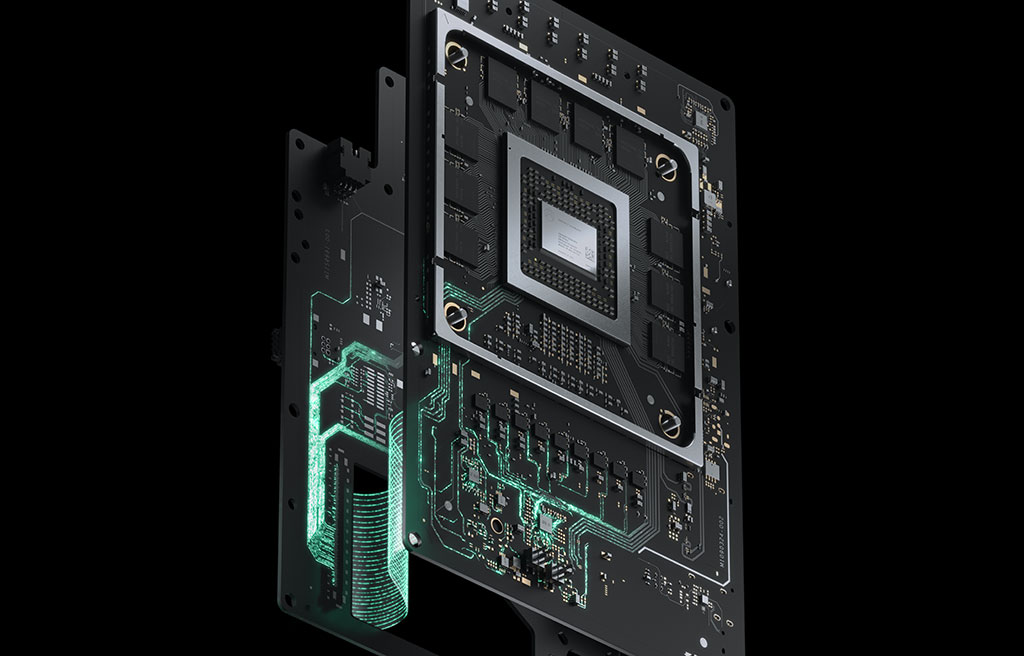
Talking about SSD's though...I just saw these official images from the Xbox website and noticed the SSD is depicted as what looks like a ~30mm x 42mm form factor and you can clearly see a 'half moon' shape screw hole like on PC cards? You can also see a ribbon cable that goes to the I/O board with the expandable storage slot in the other image. I would've thought it would be flash chips soldered direct to the PCB but maybe not?

Not hung up on the compression, just trying to keep things simple and fair. True about RD0 and the Microsoft dev on Twitter even pointed that out.
Talking about SSD's though...I just saw these official images from the Xbox website and noticed the SSD is depicted as what looks like a ~30mm x 42mm form factor and you can clearly see a 'half moon' shape screw hole like on PC cards? You can also see a ribbon cable that goes to the I/O board with the expandable storage slot in the other image. I would've thought it would be flash chips soldered direct to the PCB but maybe not?
I also thought they would have soldered it onto the board. It could be upgradable but I don't see why they didn't just solder it on.
Rusco Da Vino
Member
You did well my friend, it was all BS. A total waste of time.Okay, I'm still relatively new, so I either didn't pay enough attention to those parts or didn't read back far enough in the thread.
The only person/insider that was posting on point was
But lets move on, this matter is just disgusting.
Last edited:
- Status
- Not open for further replies.