How much of the die will be dedicated to raster then, I confess I have no clue of the size or the tensor core block, and how much bandwidth is necessary to take advantage of them, Mark Cerny talked a lot about the challenge that is keep the PSSR feed with data LPDDR is already slower than GDDR as it is. Switch 2 will feature DLSS, I believe in that, but what I'm waiting to see is how good the implementation will be giving the parameters of a handheld console.
Best answer we have is if you pack all 128 Cuda cores + 4 tensor cores per SM, cuda cores account ~70% and tensor cores ~30%, but this is all guess work, nobody is accurate in that kind of detail at this scale. I saw floating earlier in the day someone trying to guess the size of tensor cores by the white paper diagrams and that for sure is not to scale
Best we have is Ada. Close to Ampere, same 128 cuda cores & 4 tensor cores count, even if tensor core had a gen difference probably not much changes at this scale and accuracy of the guess. We're nowhere near accuracy levels that gen to gen changes we can verify.
As he says, its all a guess
~22-30% numbers have been floating for a while, but that's compared to cuda cores. In the end, in the whole SM, it's much less. closer to 8-10%.
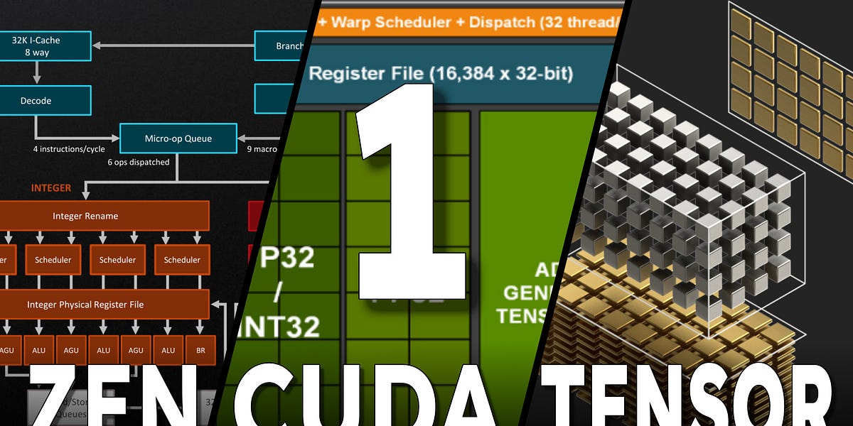
There's more in this article from the same source of the video
Given the complexity of today's computing hardware, it’s easy to get confused about what is meant by the word “core”.

www.computerenhance.com
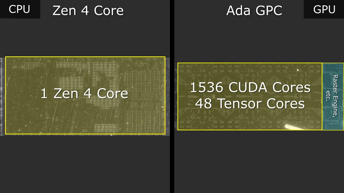
This cluster of Ada is exactly the number of cuda cores and tensor cores that Switch 2 is rumored to have, the T239. 12 SMs, 128 cuda cores + 1 RT core + 4 tensor cores per SM for a total of 1536 cuda cores, 48 tensor cores and 8 RT cores. 1 GSC of Ada takes 12 SMs though while Tegra has much less SM per GSC, making the chipset bigger than this diagram.
You then have to put ARM A78 in there, I/O, sound, video encode/decode, ISP, memory bus, etc etc. To make the APU. T239 also has a bit different setup than this Ada SoC.
Likely, but nobody knows yet... to be this kind of config, T234 seen here. 16 SM → 12 SM, 12 A78 → 8 A78.
One of the reason I don't believe it can be Samsung 8nm is that to fit exactly 12SM + 8 A78 cores, you basically are at 88% of the 200 mm^2 capacity just for the SM & core logic without anything else that makes up the APU. Fitting that in 12% of the remaining area is more than optimistic.
AND you do not have binning opportunity, so I would be highly surprised that Nintendo is going to Samsung fab and have the requirement of having perfect die without any binning for a >100M production chipset. Who the fuck is crazy enough to do that? One defect and the chip is ruined, straight to trash. That's money thrown out and slow down of production. That's money wasted. Nintendo does not like to waste money. The cost of extra SM & Cores is worth it for raising yields.


